EIKOS

Giới thiệu tổng quan

Một số tính năng được cung cấp trên EIKOS Atom Probe:

  • Chụp cắt lớp ba chiều với đặc tính kích thước nano của cấu trúc vi mô
  • Phát hiện nguyên tử đơn có độ phân giải không gian cao với hiệu quả cao
  • Độ nhạy như nhau đối với tất cả các nguyên tố và đồng vị của chúng
  • Đo lường thành phần định lượng (thang đo sub-nm đến gần micron)
  • Có sẵn trong các cấu hình điện áp hoặc điện áp & laser
  • Phương pháp chuẩn bị mẫu tiêu chuẩn

EIKOS có sẵn trên 2 cấu hình:

EIKOS

Hệ thống EIKOS cơ sở kết hợp thiết kế tấm phản xạ để cung cấp khả năng phân giải khối lượng tuyệt vời và tín hiệu nhiễu. Một điện cực đếm tích hợp được căn chỉnh trước đảm bảo dễ sử dụng và độ tin cậy cao. Hệ thống xung điện áp cung cấp chất lượng dữ liệu rất cao trên nhiều ứng dụng luyện kim.

EIKOS-UV

Hệ thống EIKOS-UV được định cấu hình đầy đủ kết hợp tất cả các tính năng nổi bật của EIKOS cơ sở (xung điện áp, chức năng dựa trên phản xạ, điện cực đếm được căn chỉnh trước) và bổ sung mô-đun xung laser 355 nm được tích hợp đầy đủ với thiết kế điểm tập trung được điều khiển bằng máy tính để cung cấp quyền truy cập vào hệ thống lớn hơn. phạm vi ứng dụng.

Hệ thống EIKOS cơ bản có thể nâng cấp lên EIKOS-UV.


Product overview

The EIKOS Atom Probe offers:

  • Three-dimensional tomography with nanoscale characterization of microstructures
  • High spatial resolution single atom detection with high efficiency
  • Equal sensitivity to all elements and their isotopes
  • Quantitative composition measurement (sub-nm to near micron scale)
  • Available in voltage or voltage & laser configurations
  • Standard specimen preparation methods


EIKOS is available in 2 configurations:

EIKOS
The base EIKOS system incorporates a reflectron design to provide excellent mass resolving power and signal to noise. A pre-aligned integrated counter electrode ensures ease of use and high reliability. The voltage pulsing system provides very high data quality on a wide variety of metallurgical applications.

EIKOS-UV
The fully configured EIKOS-UV system combines all the outstanding features of the base EIKOS (voltage pulsed, reflectron based functionality, prealigned counter electrode) and adds a fully integrated 355 nm laser pulsing module with computer controlled focused spot design to provide access to a larger application range.

The base EIKOS system is field upgradable to the EIKOS-UV.

Characterizing grain boundaries with LEAP Atom Probe

Grain boundary analysis in metals (APT)

The LEAP 5000 and EIKOS Atom Probes offer unique capabilities for nanoscale chemical analysis and 3D imaging of grain boundaries in metals and alloys.

Keep Reading

Nanoscale characterization of phase change materials with Atom Probe Tomography

Investigation of phase change separation processes (APT)

Thanks to unique spatial resolution capabilities, CAMECA Atom Probes can investigate phase separation processes in energy storage materials.

Keep Reading

  • Introduction to applications & technology of EIKOS-UV

    Optimized or efficiency and simplicity, EIKOS-UV™ delivers all the benefits of Atom Probe Tomography and addresses a wide range of applications: metals, coatings, thin films, ceramics, minerals, functional materials in both academic and commercial environments. Robert Ulfig (CAMECA) presents the main features and functionalities of CAMECA's latest atom probe tomography instrument.
    Register here to view at any time.
    ↓ Duration: 23 minutes

    Click here to view

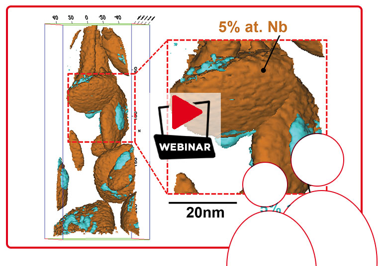
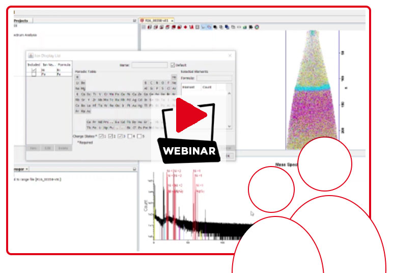
  • An Introduction to IVAS LT

    If you have atom probe data, and are looking for an efficient and free method to conduct analyses, check out IVAS LT. This free version of IVAS software allows you to conduct a number of different tests on your data. Learn more by watching this free, short webinar, and then download your copy of IVAS LT!
    ↓ Duration : 19 minutes

    Click here to view

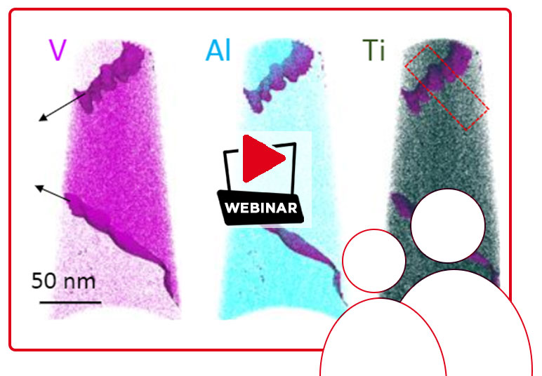
  • Atom Probe Tomography for Additive Manufacturing Part 1

    Intro to AM Methods and Maraging Steel Case Study Deals with maraging steel. Click the link to watch this short webinar with a Q&A session.
    ↓ Duration : 23 minutes

    Click here to view

A selection of Atom Probe Related Web Sites

International Field Emission Society (IFES)
The International Field Emission Society is an international scientific society, that aims to promote high field nanoscience and atom probe microscopy. At each IFES Symposium, organised every 2 years, the E.W. Müller Outstanding Young Scientist Award is given to the best orally-presented paper in a competition.

Materials Physics Group, Rouen University, France
The GPM is a joint University of Rouen-CNRS and INSA research unit led by Prof Didier Blavette. It is one of the largest groups of the atom probe community. CAMECA collaborates with GPM for the design and development of its atom probes.

Oak Ridge National Laboratory, Microscopy Group, USA
The Microscopy Group at ORNL specializes in the development and application of advanced electron microscopy, atom probe tomography, and surface science techniques for the sub-nm scale characterization of the microstructure, chemical nature, and composition of materials. Equipped with a CAMECA LEAP, scientists and engineers at ORNL greatly contribute to the advancement of 3DAP technology and applications.

Geoscience Atom Probe, Curtin University, Australia
The development of the Geoscience Atom Probe as part of the Advanced Resource Characterisation Facility, housed in the John de Laeter Centre at Curtin University, provides a unique focus on the development and application of this exciting technique to the Earth Science discipline.

Northwestern University Center for Atom Probe Tomography (NUCAPT), USA
The Seidman Research Group at Northwestern University, Illinois, uses a LEAP 4000X Si to study the chemical composition and evolution of precipitates, interfaces, and other nanoscale phenomena. The Seidman Group ranks among the top research teams involved in the investigation of nano-structured materials.

Marquis Research Group, University of Michigan, Ann Arbor, USA
Part of the Department of Materials Science & Engineering of the University of Michigan, and equipped with a LEAP 4000X-HR, the Marquis Research Group focuses on the experimental exploration of the atomic scale structures to understand materials behavior and develop more efficient materials and structures for energy applications.

FIM & Atom Probe Group, Department of Materials at Oxford University, UK
Over more than 40 years of history, the Oxford FIM and Atom Probe Group have been world leaders in the development of the atom probe technique and its application to materials science problems.

ACMM, University of Sydney, Australia
The Australian Centre for Microscopy & Microanalysis (ACMM) is the University of Sydney’s centralised microscopy facility. Directed by Prof. Simon Ringer, it provides Sydney’s research community with leading instruments and expertise for exploring the structure of samples, from physical to biological and everything in between, at length scales down to the molecular and atomic.

Deakin University, Electron Microscope Facility, Victoria, Australia
Housed in the Geelong Technology Precinct at the Geelong Waurn Ponds Campus, Deakin Electron Microscope Facility supports a wide range of research projects that lead and inspire innovations in materials science and engineering.

Metallic Nanostructure Group of NIMS, Japan
Dr. Hono's Atom Probe group is part of the Materials Engineering Laboratory within the National Institute for Materials Science (NIMS) in Tsukuba, Japan.

Max-Planck-Institut für Eisenforschung, Düsseldorf, Germany
MPI Düsseldorf's Atom Probe Tomography Group, under leadership from Dr. Pyuck-Pa Choi, conducts basic research on the mechanical properties of materials and their relationship to the underlying nano- and microstructures. It was established in 2009 in conjunction with the installation of a LEAP 3000X HR. MPI Dusseldorf is also one of the first owner of a LEAP 5000 latest generation atom probe.

Microscopy and Microanalysis group, Chalmers University, Sweden
Research projects conducted by the Microscopy and Microanalysis group aim at developing and improving a fundamental understanding of the fine-scale microstructure of technologically important materials, its manipulation and importance in determining the properties of materials.

EMEZ - Electron Microscopy, Federal Institute of Technology, Zurich, Switzerland
EMEZ is an interdisciplinary facility of ETH Zurich supporting vital research efforts and services for ETH members and visiting researchers as well as industry.

POSTECH, Korea
Pohang University of Science and Technology and National Center for Nanomaterial Technology (NCNT), under the leadership of Prof. Chan Gyung Park (pages in Korean).

Thompson Research Group, University of Alabama, USA
Professor Thompson’s research group addresses processing-microstructure-property interdependence by investigating phase transformation and phase stability in a variety of material systems at different length scales.

Montanuniversität Leoben, Austria
Dr. Francisca Mendez-Martin's team within the Department of Physical Metallurgy and Materials conducts studies in a wide field of topics: surface engineering, phase transformations, in-situ monitoring of microstructural changes during solidification and heat treatment of metallic materials, development of nanostructured material...

King Abdullah University of Science and Technology (KAUST), Saudi Arabia
Inaugurated in September 2009, KAUST has an impressive program to develop one of the world’s leading scientific research institutions. 2 of CAMECA's new generation Atom Probe models will be installed at one of KAUST's core research facility within the Materials Science & Engineering department, under leadership of Prof. Tala‘at Al-Kassab.

Fraunhofer Center for Nanoelectronic Technologies, Dresden, Germany
Located within the “Silicon Saxony”, Fraunhofer CNT provides ideal collaboration opportunities for research institutes and material/equipment manufacturers in the field of nanoelectronics. The LEAP 3000X installed at Fraunhofer CNT is dedicated to research in semiconducting materials, as well as hard coating, metallic glasses, and nuclear fusion materials.

Université Paul Cézanne, Marseille, France
The Reactivity and Diffusion at Interfaces Team under leadership from Dominique Mangelinck is part of IM2NP, a research institute supporting a wide range of programs including modelling, design, architecture, processes, materials and their physico-chemical properties.

UCSB's Materials Department, Santa Barbara, California USA
Widely recognized as one of the top materials research facilities in the world, UCSB' s Materials Department serves as the innovation engine for discoveries in new materials. Under leadership from Professor James S. Speck, it is equipped with a LEAP 3000X.

Atomprobe.com
Hosted by CAMECA Instruments Inc., the Atom Probe Tomography user's website provides APT users and system owners with a single place to get and share information.

  • AP Suite 6

    AP Suite 6

    The Atom Prober's Toolkit for Data Analysis Workstations: a user-friendly, collaborative platform to seamlessly manage your entire Atom Probe Tomography research projects within one single environment.

    Keep Reading

  • IVAS Software

    IVAS

    Specifically developed for the CAMECA Atom Probes, IVAS provides powerful visualization and analysis features to extract 1D, 2D and 3D quantitative information collected on APT instruments, quickly and easily.

    Keep Reading

Options for LEAP®

Integrated Plasma Cleaner
A fully-integrated, automated plasma cleaner offers both increased productivity and reduced cost of ownership for the LEAP system.

Residual Gas Analyzer
Allows partial pressure analysis of LEAP instrument. 

LEAP 5000 VCTM
The Vacuum and Cryo Transfer Module (VCTM) enables specimens to be transported between LEAP and ancillary workstations while maintaining both UHV and cryogenic conditions. The module utilizes a UHV-compatible portable chamber which is fully integrated (via a docking station) into the LEAP 5000. Note that the additional workstations must also be compatible with the VCTM and this is not included with this option. Please contact CAMECA sales for more details.

Productivity Enhancement Package
Extends the storage capacity of the LEAP system and includes a fully-integrated in situ heated carousel to reduce pump down times, increase specimen throughput and improve vacuum quality.

Anti-vibration Package
Active vibration isolation platform allowing the LEAP to be installed in environments not meeting vibration standards, this integrated solution combines active vibration cancellation together with an upgraded LEAP platform. Patented piezoelectric Technology cancels floor vibration in real time with active bandwidth starting at 0.6Hz.

Seismic Kit
Factory-fitted seismic restraint kit. Floor requirements must be met for purchase of this option.

Field-Ion-Microscope (eFIM) Module
Adds Field-Ion-Microscope (FIM) capability to LEAP system

Options for LEAP® and EIKOS™


Manual Electropolisher

The manual electropolishing unit is designed to allow maximum flexibility for production of specimens from a wide variety of materials. The item includes power supply, chemical handling and all accessories required to prepare high quality atom probe specimens. (Optical microscope and Chemical reagents are not included.)

Adv sample prep kit
Advanced specimen preparation kit includes key components required for advanced FIB-based specimen preparation.

  • Chia sẻ qua viber bài: EIKOS
  • Chia sẻ qua reddit bài:EIKOS

PRODUCTS

Loading...

RELATED PRODUCTS

SEM5000Pro Field Emission Scanning Electron Microscope

SEM5000Pro Field Emission Scanning Electron Microscope Manufacturer: CIQTEK – China Model: SEM5000Pro Country of Origin: China High-resolution, low-voltage imaging is enabled by CIQTEK’s “Super-Tunnel” electron optics, which eliminate beam crossover and utilize electrostatic-magnetic combined lens design. This minimizes charging effects, aberrations, and ensures 1.2 nm resolution at 1 kV for effective imaging of non-conductive and semiconductor samples with minimal beam damage.
Xem thêm

BC43 CF benchtop confocal microscope

The Andor BC43 is a compact, benchtop multimodal imaging system. It is an "all-in-one" solution featuring an integrated anti-vibration mechanism and a light-tight lid, allowing it to operate in a standard laboratory environment without the need for a darkroom or an optical table. The BC43 is positioned as a powerful yet accessible instrument that does not require deep microscopy expertise, making it ideal for core facilities. Notably, the system is in-field upgradable, providing a growth path from widefield to confocal and super-resolution imaging to evolve with research needs.
Xem thêm

NANOS SEM

The NANOS tabletop SEM offers high quality imaging at a low cost of ownership with integrated energy dispersive spectroscopy (EDS) for rapid elemental analysis. It is designed for easy installation, ease of use and easy servicing.
Xem thêm