Jacomex G[SAFE] - High Security Glove Box for Hazardous Materials
Specialized glove box for handling toxic substances, hazardous powders, or pathogens. Operates under negative pressure with dual HEPA filtration for total safety.
Xem thêmQuantitative analysis of thin films, coatings, and buried layers down to sub-atomic equivalent thicknesses and dopants at 10^14 atoms/cm^2 can be obtained through standard-less fundamental parameters or with standards. Thickness variations at the microns-scale can be determined.
The AttoMap provides unprecedented sensitivity of sub-femtogram (and sub-ppm) to measure the distribution of multiple elements simultaneously. Applications include: rare earth elements in geological samples, nanoparticles (e.g. 50-100 nm), metallomics, forensics, contaminants in advanced materials, and more.
Measurements and elemental imaging to determine co-location of trace-level minerals and rare earth elements at ppm-scale is possible at microns-scale
Elemental composition and their relative percentages can be obtained for both point analysis and for larger regions, including specific regions of interest or the complete sample. Data is acquired and stored as a hypermap, with each pixel and its spectra, for ultimate flexibility in analysis.
HOW DOES THE ATTOMAP ACHIEVE ITS SUPERIOR PERFORMANCE?
The AttoMap features key innovations in its:
Mineralogy
Automated mineralogy using scanning electron microscope (SEM) has become a dominant approach used in natural resource exploration and process monitoring. AttoMap provides a powerful complement to SEM-based mineralogy approaches by providing 1000X the sensitivity of SEM-EDS for trace elemental mapping. The system’s intuitive software provides AI-based grain segmentation and mineralogical identification.

Life Sciences and Metallomics
AttoMap was originally designed for life science research with support of NIH funding. Applications in the life sciences include studying pathologies (e.g., cancer and Wilson’s Disease) that are hypothesized to be related to dysregulation of trace elements such as iron and copper, the distribution of nanoparticle-based therapeutics after injection, and environmental uptake of contaminants.

Semiconductor
AttoMap has been adopted by leading semiconductor companies for monitoring dopants and ultrathin films on test patterns. The system also provides trace-level measurements of organic contaminants and low atomic number (Z) materials such as B within its vacuum environment. Pattern recognition based software enables unsupervised, recipe-based acquisition of points for high efficiency.
For backend packaging, AttoMap provides high throughput metrology of micropillar dimensions, quantification of voids in microbumps, and rapid identification of defects.

Environmental / Botany
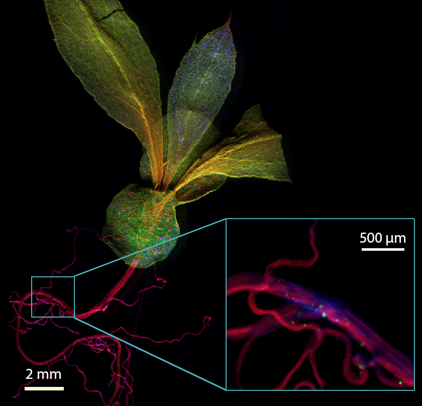
Synchrotron XRF has become a technique of choice for many plant scientists for understanding element distribution. Such studies include metal uptake for photoremediation (reclaiming the environment), nutrient uptake, and genetically modified plants for desirable characteristics such as drought-resistance and improvement to nutritional content.
| Parameter | Specification | |
|---|---|---|
| Overall | Spatial Resolution | Down to 3-5 μm with high resolution optic. 7-10 μm with standard optics. |
| Sensitivity | Sub-ppm relative detection sensitivity. Picogram to femtogram absolute sensitivity. | |
| Source | Type | Sigray patented ultrahigh brightness sealed microfocus source |
| Target(s) | Up to 5 targets. Includes selection from Si, Cr, Cu, Rh, W, Mo, Au, Ti, Ag. Others available upon request. | |
| Power | Voltage | 50W | 20-50 kVp | |
| X-ray Optic | Type | Sigray proprietary double paraboloidal x-ray mirror lens |
| Transmission Efficiency | ~80% | |
| Magnification | 1:1 magnification default Optional demagnifying optics for higher resolution | |
| Interior Coating | Platinum for increasing collection efficiency of optic | |
| X-ray Detector | Type | SDD Detector |
| Energy Resolution | <129 eV at Mn-Ka | |
| Dimensions | Footprint | 54" W x 65.5" H x 38.5" D |
| Stage Travel | 200 x 200 mm standard 300 x 300 mm for semiconductor wafers | |
| Maximum Sample Size | 300 x 300 mm | |
| Additional Capabilities | Other Modalities | Integrated optical microscope and transmission x-ray microscope for alignment |
| Software | Sigray Composition (GUI-based analysis tool) Semiconductor Acquisition Jupyter notebooks available upon request |