Atom Probe Tomography EIKOS

The Atom Probe that enables routine, high performance 3D nano-analysis for both research and industry. Building on 30 years of success in Atom Probe Tomography (APT) instrumentation and application, CAMECA announces EIKOS-UV™, the Atom Probe Microscope that brings APT to the next  generation of material scientists, metallurgists, physicists, geologists and engineers.

EIKOS-UVTM: Accessible APT
The new EIKOS-UV™ provides excellent analytical performance from a platform optimized for both efficiency and simplicity of operation. EIKOS-UV™ delivers all of the benefits of APT - nanoscale characterization of materials with the best combination of high spatial resolution and detection sensitivity - in an easy to use, affordable package.


The EIKOS Atom Probe offers:

  • Three-dimensional tomography with nanoscale characterization of microstructures
  • High spatial resolution single atom detection with high efficiency
  • Equal sensitivity to all elements and their isotopes
  • Quantitative composition measurement (sub-nm to near micron scale)
  • Available in voltage or voltage & laser configurations
  • Standard specimen preparation methods


EIKOS is available in 2 configurations:

EIKOS
The base EIKOS system incorporates a reflectron design to provide excellent mass resolving power and signal to noise. A pre-aligned integrated counter electrode ensures ease of use and high reliability. The voltage pulsing system provides very high data quality on a wide variety of metallurgical applications.

EIKOS-UV
The fully configured EIKOS-UV system combines all the outstanding features of the base EIKOS (voltage pulsed, reflectron based functionality, prealigned counter electrode) and adds a fully integrated 355 nm laser pulsing module with computer controlled focused spot design to provide access to a larger application range.

The base EIKOS system is field upgradable to the EIKOS-UV.

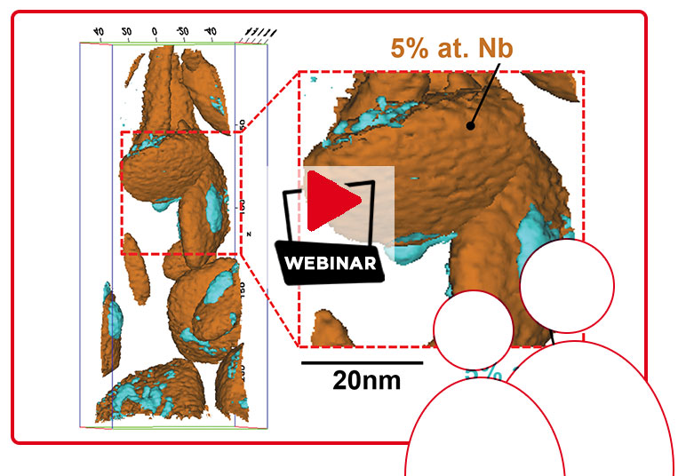
Characterizing grain boundaries with LEAP Atom Probe

Grain boundary analysis in metals (APT)

The LEAP 5000 and EIKOS Atom Probes offer unique capabilities for nanoscale chemical analysis and 3D imaging of grain boundaries in metals and alloys. 

Keep Reading


Nanoscale characterization of phase change materials with Atom Probe Tomography

Investigation of phase change separation processes (APT)

Thanks to unique spatial resolution capabilities, CAMECA Atom Probes can investigate phase separation processes in energy storage materials. Keep Reading


An Introduction to Atom Probe TomographyAPT Intro

Looking for a brief overview of the technique? Perfect for sharing with researchers just starting in APT.


Grain boundary analysis in NdFeB with Atom Probe Tomography and t-EBSD

Grain boundaries in NdFeB alloy - 3D Atom Probe data combined with t-EBSD

The grain boundaries visible in the tEBSD data show copper segregation (orange dots) and a NdO precipitate (gray dots). Combining crystallographic data with 3D APT data provides for a more complete picture of the material.


Introduction to applications & technology of EIKOS-UV

Optimized or efficiency and simplicity, EIKOS-UV™ delivers all the benefits of Atom Probe Tomography and addresses a wide range of applications: metals, coatings, thin films, ceramics, minerals, functional materials in both academic and commercial environments. Register here to view at any time. Click here to view

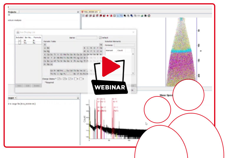
An Introduction to IVAS LT

If you have atom probe data, and are looking for an efficient and free method to conduct analyses, check out IVAS LT. This free version of IVAS software allows you to conduct a number of different tests on your data. Learn more by watching this free, short webinar, and then download your copy of IVAS LT! Click here to view

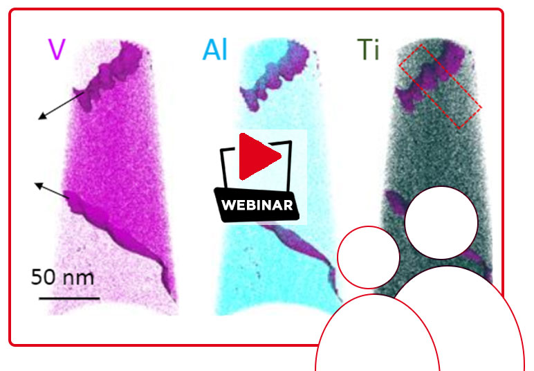
Intro to AM Methods and Maraging Steel Case Study Deals with maraging steel. Click the link to watch this short webinar with a Q&A session.
Click here to view


Please click to view additional webinars


  • Chia sẻ qua viber bài: Atom Probe Tomography EIKOS
  • Chia sẻ qua reddit bài:Atom Probe Tomography EIKOS

PRODUCTS

Loading...

RELATED PRODUCTS

Hệ thống Quang khắc không mặt nạ đầu dò nhiệt NanoFrazor

NanoFrazor dùng công nghệ khắc nhiệt không mặt nạ (t-SPL) với đầu dò siêu nhọn, tạo cấu trúc nano chính xác cao, không cần chùm điện tử hay mặt nạ đắt tiền. Độ sâu khắc sai số <1nm, tích hợp kiểm tra in-situ, hỗ trợ grayscale 3D cho quang tử nano, cảm biến lượng tử, màng sinh học. Module Decapede 10 đầu dò giúp tăng thông lượng gấp 10 lần.
Xem thêm

Maskless Lithography System DWL 2000 GS / DWL 4000 GS - Heidelberg Instruments

The DWL 2000 GS / 4000 GS meets industrial standards, supporting CAD export with up to 1023 grayscale levels. Proprietary Grayscale technology from Heidelberg Instruments enables the fabrication of 2.5D structures and microlenses with surface roughness down to 5nm. An optimal solution for manufacturing holograms, light diffusers, and Fresnel lenses in nanophotonics and micro-optics research.
Xem thêm

Maskless Lithography System DWL 2000 GS / DWL 4000 GS - Heidelberg Instruments

The DWL 2000 GS / 4000 GS meets industrial standards, supporting CAD export with up to 1023 grayscale levels. Proprietary Grayscale technology from Heidelberg Instruments enables the fabrication of 2.5D structures and microlenses with surface roughness down to 5nm. An optimal solution for manufacturing holograms, light diffusers, and Fresnel lenses in nanophotonics and micro-optics research.
Xem thêm

UPDATE

WE HAVE MOVED TO
WWW.adst.vn

THANKS FOR YOUR VISIT OUR NEW WEBSITE!

VISIT NOW